
PCB Design is the art and science of creating a 2d Design for electronics circuit which can be fabricated on a board.
If you’re anyway related to electronics, either a hobbyists, or an engineering student, or someone who’s currently working in the field of electronics, then its almost impossible that you don’t know about PCB Design
As said PCB stands for Printed circuit board. Whenever we have a circuit on paper, and we want to test it or build physical format of that circuit then we build a printed circuit board. So basically PCB is a solid format of a circuit which is drawn on paper. And to design the PCB we need to understand about the electronic circuit and its interactions properly. That’s why it said that PCB design is an art as well as a science at the same time. A designer must consider number of different parameters but most important of them are the size of PCB and the number of components mounted onto it. A good PCB design is one which can accommodate more components in less area Hey at the same time not giving any Hey unconnected traces.
PCB Design or printed circuit board design is the process of giving a solid form to a circuit we create on paper. Usually we can prototype any circuit using a breadboard. On a breadboard you can very well test a circuit but to create a physical circuit you need to design PCB’s. learn more about breadboards here Short form of Printed Circuit Board is what we commonly call as PCB. PCB Design is an art and science at the same time, because, you need to know about the electronic components, their current flow and related things in order to design PCB and, you must be artistic enough to make your pcb look good. You might have heard about the Steve Job’s obsession about making things beautiful inside a computer, and it also involved, how the PCB’s looked, and how the tracks bent on the board 🙂
What are the major steps in PCB Design to know?
For anyone to be able to design PCB’s, few things are important to be known first which are
- Familiarity with Electronics Components
- Understanding of PCB Footprint which is also called as package
- Understanding of Copper Sides in the PCB that you’re using, single or double sided
- Component Placement, proper component placement is most crucial in designing boards
- Routing, you need to know the requirements of current to flow from the PCB tracks that you’re going to design, what are the requirements, and whats the relation between track size and the maximum current it allows to flow
How PCBs are Designed?
PCB Design, in old days, was mostly done on paper, where one has to just draw the Artwork on paper, usually a graph paper to get proper idea of dimensions and then place the component footprints on the paper by drawing them. Last step was to interconnect those components using tracks drawn simply with pencil. In many academic institutes, this is the primary step of how PCB design is taught to students and its for the better because you get the core concept of it when learning it for the first time.
Initially, everyone learns about single sided PCB’s where there’s copper only on one side of PCB and over time, the PCB design learning becomes much more complex when we know about creating a dense PCB in a small size. So then comes double sided PCBs where there is copper on both sides, so designer can place components as well as route tracks from both sides of PCB. And from this time and on, most designers shift to using Computer Aided Tools for PCB Design (CAD)
What are popular CAD PCB Design tools?
There are many PCB design tools available in market, many of them are free, many of them are paid versions. And selection of the PCB design tool completely depends on what suits best for your requirement. Am just giving few names here based on how popular they are and how costly the are, but offcourse, there’s much more than this list
- Mentor Graphics PADs, perhaps the most expensive PCB Design tool used by many corporate product design companies
- Proteus Design Suite, more preferable due to both PCB design and electronics simulations that comes under single package
- Altium(previously protel) provides a complete design suite with 3D visualization and overview about how PCBs will fit into its enclosure
- OrCAD one of the oldest software
- Eagle undoubtedly, eagle pcb design software can be called as the most dominant and most popular tool because its used by both industries and hobbyists community around the world, and with flexible pricing, its affordable for even a single person startup
- KiCAD one of the most popular 100% free PCB design tool
- EasyEDA complete cloud based 100% free online and powerful pcb design tool
The list goes on and on and its just based on trials and erros that you’ve to chose the tool appropriate for you
Download-NowImportance of Learning PCB Design
If you’re a student studying engineering or someone who is willing to start his own startup, its very important to understand and learn at least the basics of PCB design. As engineering student, knowledge of basic single sided PCB design is something kind of compulsory thing to know about. You can download any of the above software or try easyEDA directly on cloud without downloading the software on your computer and start experimenting with it right away
Now, we all know that the most developments, everyday are happening in the field of electronics, there are new mobiles, new IoT devices, and lots of new gadgets and researches going on, and all of this needs product design which involves PCB design as primary skill. And in the era of Arduino’s and Raspberry Pi, its easier to find a programmer or embedded developer but day by day, its getting difficult for startups to find a good PCB designer, why? because people are simply ignoring studying PCB designs.
Which software to choose?
Whether you’re a student looking for job or a hobbyists who wants to make nice fun projects for himself for the coming weekend, learning PCB design by choosing appropriate tool becomes very important. My personal suggestions is not only one but I’ve 2 recommendations. The recommendations are based on very simple parameters
- Popularity (eagle is one of the most popular one)
- Cost (easyEDA is by far the best completely FREE pcb Design suite I’ve ever used)
Eagle (download here)
Choose eagle if you either plan to start a company in future, or wants to design hobby circuits which are small one. These are 2 ends of a string. Because eagle free version allows a fairly small size of PCB to be designed so it should fit only small circuits and eventually you might want to buy it.
But the benefit with eagle is immense, first of all, its a completely powerful tool with all the features you might need, secondly, almost every open source hardware design available on internet is made using Eagle, so adaptation is easier,a complete guide on eagle
- Free limited version is available
- Very popular
- Large user libraries available for almost every part to be used
- Number of open source projects made in eagle, makes it easy to adopt
- Very little learning curve
- Small size installation
For those interested in knowing the basics of Printed Circuit Board design, here’s my explained video which will create most of the doubts for beginner
Download-NowEasyEDA (Download or use here)
If you’re comfortable using a completely cloud based software where all your designs are also saved on cloud, then easyEDA is one of the best choices because of many reasons,learn here a complete guide
- Its Free
- Takes no installation, runs on cloud
- Optionally you can run it on your local machine but its totally optional
- Learning curve is simple, I mean dead simple, probably 1 hour
- User contributed parts library is huge, large, gigantic I’d say 🙂
Based on these 2 things, you can choose whichever is best for you after experimenting.
For those interested in knowing the basics of Printed Circuit Board design, here’s my explained video which will create most of the doubts for beginner
What Is PCB made of?

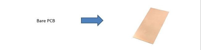
A PCB is made up of a thin board which is having copper deposited on one or both sides of the board. The board is usually made up of a non-conductive material. The board is usually having a thickness which where is from 0. 6 MM to 2 mm. the most popular board size is 1.6 mm. The thickness of copper deposited onto it varies widely but the standard thickness is 35 micron. However we have used PCBs where we wanted up to 100 micron thickness. The thickness of copper layer is directly proportional to the current the copper layer can conduct. When we need the same size copper layer to carry more current, in that case we choose to increase the layer thickness instead of completely redesigning PCBs. In single sided board, we have copper deposited on only one side. In double sided PCB, copper is deposited on both the layers of board. A bare PCB looks like this.
There are variety of materials with which the board is made up of. However a comprehensive list for reference is available here. This material is called as substrate. Usually, the most widely used substrate is a fiber glass or also a code name FR-4. This solid core gives the PCB its strength. Depending upon requirement, flexible PCBs can also be made. In the case of flexible PCB, the substrate is made up of high temperature plastic.
Copper layers can be of different thickness Most common and popular thickness of copper layer is 35 micron
Substrate
The base material or substrate, is usually fiberglass it’s called “FR4”. This solid core gives the PCB it’s rigidity and thickness. There also flexible PCB’s built on flexible high temperature plastic(Kapton or the equivalent).Board thickness 0.8mm-2.6mm thickness, most common is 1.6mm thick board
What is the process of PCB manufacturing?
The steps of PCB manufacturing can be summarized as
- Schematic Capture: Drawing the Circuit diagram of required PCB
- Draw PCB Layout and Artwork: The process of creating a layout of components on an expected size and then interconnecting the components using tracks. This is a drawing stage and usually done on computer using suitable software.
- DRC: Once the design is completed, we need to perform a design rule check to see if there are any errors
- Export Gerber: In this step we export the manufacturing data from the PCB Design software. This data is then sent to manufacturer
- Drilling: Manufacturer, first drills your entire PCB
- Etching: in this step, the PCB design is drawn on the PCB and it undergoes a process called etching. In etching process, the unwanted copper is removed using a chemical reaction with a suitable chemical like ferric chloride. After etching, PCB contains only the copper which is needed for tracks and all unwanted copper is removed.
- Printing: The additional colour mask, text layer and every thing needed is printed in this step
- Shipping: once its done, the PCBs are cut depending upon requirement and shipped to the customer.
DIY vs Manufactured

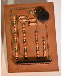
There is a significant difference between the quality of a do-it-yourself PCB and the one which is manufactured by a PCB manufacturer. You can make your own PCB’s for single sided PCB’s without any complex machinery with you. But the same is not possible for a double-sided PCB. The DIY PCB is made by printing the layout using a laser printer on a photo paper and then transferring that to PCB using Hot iron. The etching can be done at home by simply making a solution of FECL3 chemical. But when it comes to long life operation, its always preferred to get the PCB’s manufactured from a known standard manufacturer.
The DIY PCB looks like this:
and the manufactured PCB looks like this
Solder Mask and Silk Screen
When you manually make PCBs at home, you can not have the solder mask and silk screen on PCB. Solder mask is the nice attractive Green/red/black/blue colour which appears on a PCB when we look at it. The silk screen is the white borders around the components and the labels of the components are also printed using the same white ink. We call this as silk screen. Since these prints needs a very fine adjustment between the printing mechanism and PCB itself, it’s really difficult to make them at home. Even if you have a screen-printing setup at home, its still not an easy task to print them on PCB.
Solder Mask
Silk Screen

Download-Now
Common Terms
DRC–> Design rule check
Hole–> Hole to insert and solder component
Pad–> Pad to solder surface mount component
Via–> Hole to connect 2 layers of PCb
Track–> Copper line connecting 2 parts / wire of circuit
Jumper–> Wire to place where track can’t be drawn
Plane–> Excess copper area
Foot print–> Component print on PCB
Measurement units on PCB
Generally all PCB design softwares support multiple measurement units to make it easier for all the designers across the world. There are few measurement units which are supposed to be very standard in PCB Design softwares. And the unit is called as th or thou
And its a good practice to understand about the thou. Its nothing but one thousandth of an inch. So its easier to remember as well.
1 th == thou == 0.001 inch = 0.0254 mm =0.00254 CM
thou is the most common unit in PCB design tools, However mm can also be used.
Popular dimensions offered by PCB design softwares
- thou also specified as th
- mm
- cm
- inch
Single Sided PCB Design and double sided PCB Design
When we’re creating a simple circuit, usually all the components are placed on one side of the board and the tracks appear on the opposite side of the board. This type of PCB design is called as Single Sided PCB Design. This is most common among the developers and hobbyists. The biggest benefit of using single sided PCB, is the ease of design. Anyone can develop a small single sided Design on Paper also. Further more the projects having less number of components can be designed using PCB
But the disadvantage of Single sided PCB comes forth when we’re trying to create a complex circuit in a restricted format. In that case, a single sided PCB design may not fir the expected size of the board and we may need to turn to Double Sided PCB Design
Advantages of Single Sided PCB Design
- Easier to start development
- Low priced
- can be made at home
- Quick turnaround / delivery time
Disadvantages of Single Sided PCB
- Complex circuit’s cannot be built in a same space
- due to all components being on same size, usually the size of board is bigger.
Double Sided PCB
In a double sided PCB, the copper deposition is present on both the sides of the board. Due to the copper deposition on both sides, we can design circuit paths on both sides of the board. This also helps us mount components from both the sides. The 2 layers, top and bottom can be connected by “via”
Via, is a name given to a small hole on PCB which is plated thougoughly. This plated hole gives connectivity for both the layers to communicate with each other. Means if you’re routing a track on bottom copper, but now you think that some part of the route should come from the top layer of PCB, then a via is added. The via gives a conducting path between top layer and bottom layer of PCB

Advantages of Double Sided PCB Design
- Complex PCBs can be designed in a small size / package
- gives more freedom and reduces the human effort to create PCB Design
Disadvantages of Doble Sided PCB Design
- Double side PCB Design and manufacturing is expensive compared to single sided Design
- Design process is quite lengthy
- More time required to manufacture PCBs
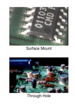
Surface Mount Vs Through Hole Components
In electronics circuit design, there are primarily 2 type of components which are available
- Through-hole
- Surface Mounted

A through hole component, as the name suggests go through a hole on PCB to the other side. The soldering action is then taken from the other side. Usual resistors, capacitors, and even IC’s like 555 or op-amp comes as through hole package by default. The electronic components used for study and experimentation are also through hole component to make it easier to insert on a bread board or soldering and de-soldering the component from PCB.

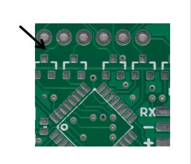
Where as SMD or Surface Mounted Device is the one which can be mounted directly on the surface of PCB. Look at the picture below
Download-Now
as you can notice, the IC is a surface mount component. It can directly be soldered on PCB and saves a lot of space because its generally very smaller than the through hole components. Whereas the through hole components shown in below picture are resistors, capacitors and many such general components which we’ve been using for a while.
Soldering a through hole component is very easier and can be done via hand without much efforts. Soldering of SMD components using bare hands can be tricky. Although it depends totally on the user’s hand, but hand soldering is not a solution for mass manufacturing and in that case a reflow soldering oven is used for all types of components.
One of the biggest advantage of through-hole components is that it provides a very strong mechanical bonds with PCB making it stronger.
Despite the fact that surface-mount technology has, by and large, replaced through-hole mounting, the through hole technique enables engineers and manufacturers to deal with components that will undergo mechanical stress as the result of this mechanical bond. As an example, connectors or heavy components like transformers are generally better suited to through-hole mounting
Having laid out as much information in as less words, its time to start your own PCB Design journey. Its completely up to you to choose the software, the PCB manufacturer and every single aspect of it. Remember you start experimenting first, and then go on refining the tools. Keep Experimenting!!!
Download-Now